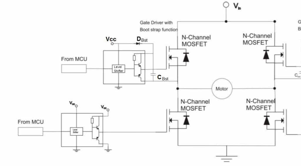
I am curious to know how the bootstrap capacitor Cbst in the following example charges up to Vcc + Vin?
https://www.homemade-circuits.com/wp-content/uploads/2019/04/bootstrapping.jpg
According to my understanding, during the clock input which turns the low side mosfet ON, the Cbst is charged at Vcc via Dbst, during the next clock the low side mosfet turns off and the high side mosfet begins turning ON through Vcc via the emitter of the NPN buffer. This allows the drain voltage to reach the source of the mosfet which simultaneously passes through Cbst via the NPN buffer to the mosfet gate. When this happens the stored Vcc inside Cbst comes in series with the instantaneous mosfet source voltage, and together they execute the Vcc + Vin for turning ON the high side mosfet.
A brief clarification on this will be greatly appreciated!
Best Answer
\$V_B\$, is the boost voltage required for dual N-channel half-bridge switches. The high output side, (HO) Nch FET needs a gate voltage higher than Vdd to activate RdsOn. It generates this voltage from a charge pump using the LO side PWM high-frequency pulses. THe Cboot cap AC couples this signal then is cathode clamped to Vdd such that the pulses now ride above Vdd. Internal to the IC, they are then rectified by an internal diode Anode and small internal capacitance to create HO +ve pulses.
The +ve current discharge pulses are shown in blue to Q1 below, while the -ve charge pulses are pulled down by Q2 to 0V.
More details Ref: https://www.onsemi.com/pub/Collateral/AN-6076.pdf.pdf