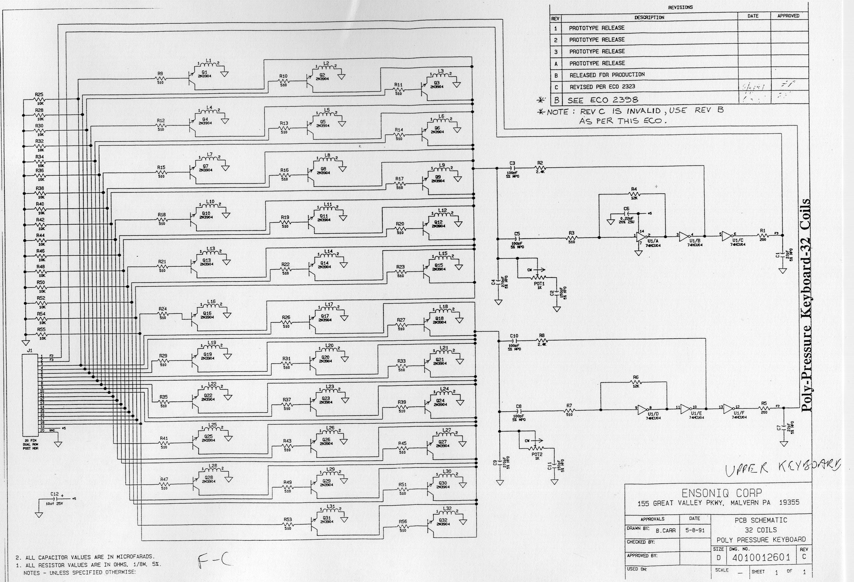
I've been looking to interface with a keyboard that I've removed from a non-functional system, specifically an Ensoniq EPS-16. As luck would have it, I managed to find schematics for the controller board, which handles the output of inductive sensors underneath the keys, and hands it on to the main controller.
I have reason to believe the controller board may be faulty (or at least, I am having a lot of trouble getting input or output from the MC68HC11 micro controller on the board) and I can not find any documentation about the proprietary IC (Motorola branded S38BC010PS01) used, processes the key output signals.
My plan is therefore to read the data directly from the keyboard signals which is where I'm having trouble. I can so far deduce that there are 4 input select lines and 4 data output lines, the input lines, CS0 to 3, drive a set of 4 to 8 demux ICs (74LS138) which select the key/bank of keys to poll data from.

From there, the output of the demux lines is fed through a strange network of transistors and the individual key inductors, and then into a bizarre use of inverter gates which are then directed to 4 output lines F0 to 3. I have no idea what kind of output signal I should be expecting. At rest, all of the output lines sit at 2.5 volts does not change if I press anything.

Everything I've described is shown in full in the schematics KBD-LOWER with the rest of the keys in KBD-UPPER. The main input/output header leads into the KPC Controller board where the micro controller and the other proprietary chip process the information.
Someone else with a similar mission to mine posted here that the output signal is a 3MHz rectangle that adjusts with key presses but I'm not seeing how it could be produced, and my only analog scope is low frequency and doesn't detect any worthwhile changes in the 2.5 volt signal
Best Answer
Firstly, get a cheap analogue 20MHz scope at least otherwise you'll have great difficulty debugging any project involving these boards. You're seeing 2.5V as the average of a 5V square wave at high frequency. (Either that or the oscillator is very broken).
simulate this circuit – Schematic created using CircuitLab
Start by examining U3/A at the center of this. Consider a DC analysis (pretend C7 does not conduct). The inverter's output is connected to its input through R19. This cannot be stable and it will tend to oscillate.
L1 is a representative inductor with its multiplex transistor turned on (not shown in diagram).
An edge from U3/A will be inverted again and fed into the LC oscillator tank L1/C6 (there's another capacitor and a tuning pot I've not bothered with). Oscillations coming out of the tank are fed back into the inverter pair through the comparatively small R18, so the LC tank pushes the inverter oscillator around rather than vice versa. Exact frequency analysis of this is going to be a pain but I suspect the delay through the inverters is roughly the period of 3MHz.
So the output at F0 is a square(ish) wave whose frequency depends on the inductance of L1, which in turn depends on the position of the key. Quite a neat bit of analogue electronics - high noise immunity and good sensitivity.
How do you read this thing? Get a moderately fast microcontroller with a timer/counter unit. Use two counters: one to count input edges, one to count elapsed time. Convert to a frequency. Measure experimentally what range of values you see across the depression of a key. Not sure whether this will be linear. Try not to use long wires and avoid solderless breadboard.
(You could also do frequency-to-voltage in the analogue domain, but that's a pain)