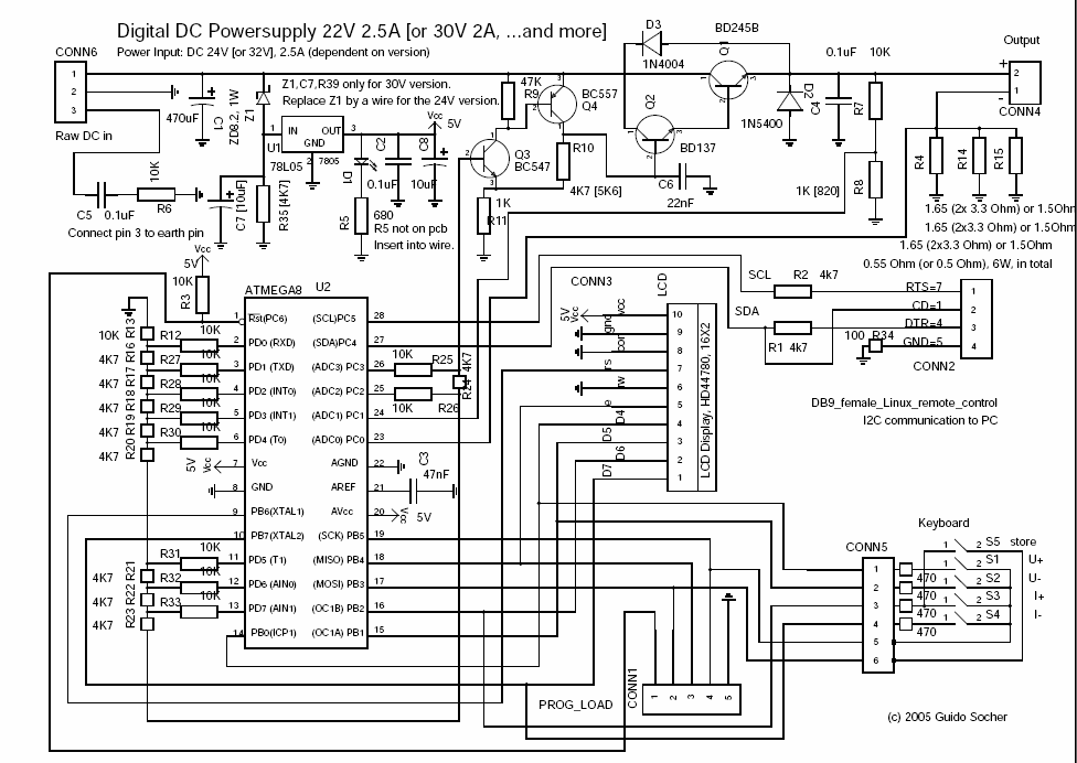
I've built this circuit: http://www.tuxgraphics.org/common/images2/article379/powersupply.gif
Here is a closeup of the amplifier section which I've built:

simulate this circuit – Schematic created using CircuitLab
And in the instructions here http://www.tuxgraphics.org/electronics/200506/article379.shtml Guido suggests a testing routine:
-
Test1: Connect some powersupply (at least 15V) to the power input of the circuit and check that you get 5V DC behind the voltage regulator.
-
Test2: Measure the output voltage. It should be 0V.
-
Test3: Connect pin 7 and pin 26 on the microcontroller with a wire (no microcontroller in the socket). You should get on the output a couple of volts less than what is used at DC input. Remove the wire and the output should go back to zero. Be sure to not cause any short circuit on the output.
I'm stuck on Test3. I get 0 volts output when I connect pin 7 (Vcc) to pin 26 (end of DAC output). I've quadruple checked all transistors and matched their pinouts and orientations. I've tried replacing a couple of them incase thats the problem. However, now I'm trying to understand a little theory to understand how to debug it with a multimeter. What voltage drops could I measure to find where the problem is? I can probably gain access to an oscilloscope of that would help, however I am dealing with fixed DC voltages so I would think a multimeter would be enough.
Best Answer
Not a nice design, alas.
Will work OKish but easy to do far better.
Vout will be ~~~= k x V_DAC - ~~~= 1.2 V
Testing:
Ensure polarity of all transistors is OK
1 x PNP (BC557) should test as if there was a conducting diode from collector to base and from emitter to base and high resistance in reverse direction.
3 x NPN (BC547, BD245B, BD137) tests as if there is a diode from base to collector and base to emitter and high resistance in opposite direction.
Then:
Set VHV to say 15V BUT really need 6 x Vin at VCC to test properly. See below. His last step is wrong.
Connect Vcc etc to pin 26. Call this Vin.
Better if Vin is in 1V to 2V range - see below.
Vpin26 = Vin
R25 rhs ~= Vin as DAC has no load - usually it will look like 2R looking upstream. With uP out it is unloaded.
Q3 base = Vin. (wire)
Q3 emitter = Q3base - ~= 0.6.
Q4 e = Vhv
Q4C = 5.7 x Q3 e due to amplifier action.
So for Vcc = 5V, Q3e =~~ 4.4V
and Q4C = 4.4 x 5.7 = 25V.
SO you want < Vcc at Vin.
Adjust Vin so Q3B = say 1v to 2V.
Then Q4C ~= 6-12V and Vout about 1.2V less.
Try that and report and we can go from there.
As a guide only:
This high quality 2:15 AM antipodean Forrest Mims lookalike cct show the basic principle of using an op amp. Vout is now sampled directly by R1 R2 and compared with V_DAC. The output will be a fixed multiple of VDAC and "stiff" - it won't wave in the breeze under load as at present.
There are better way to drive an output stage but that can come later if desired. At present the output cannot get within about 2V of Vhv.
In most cases PWM could be used instead of the DAC (1 pin on uP). A 2 op amp stage filter would help it settle faster than otherwise - the LM358 shown has 2 x opamp sections and its companion LM324 has 4. I realise you probably have a PCB for this so major changes are not attractive.