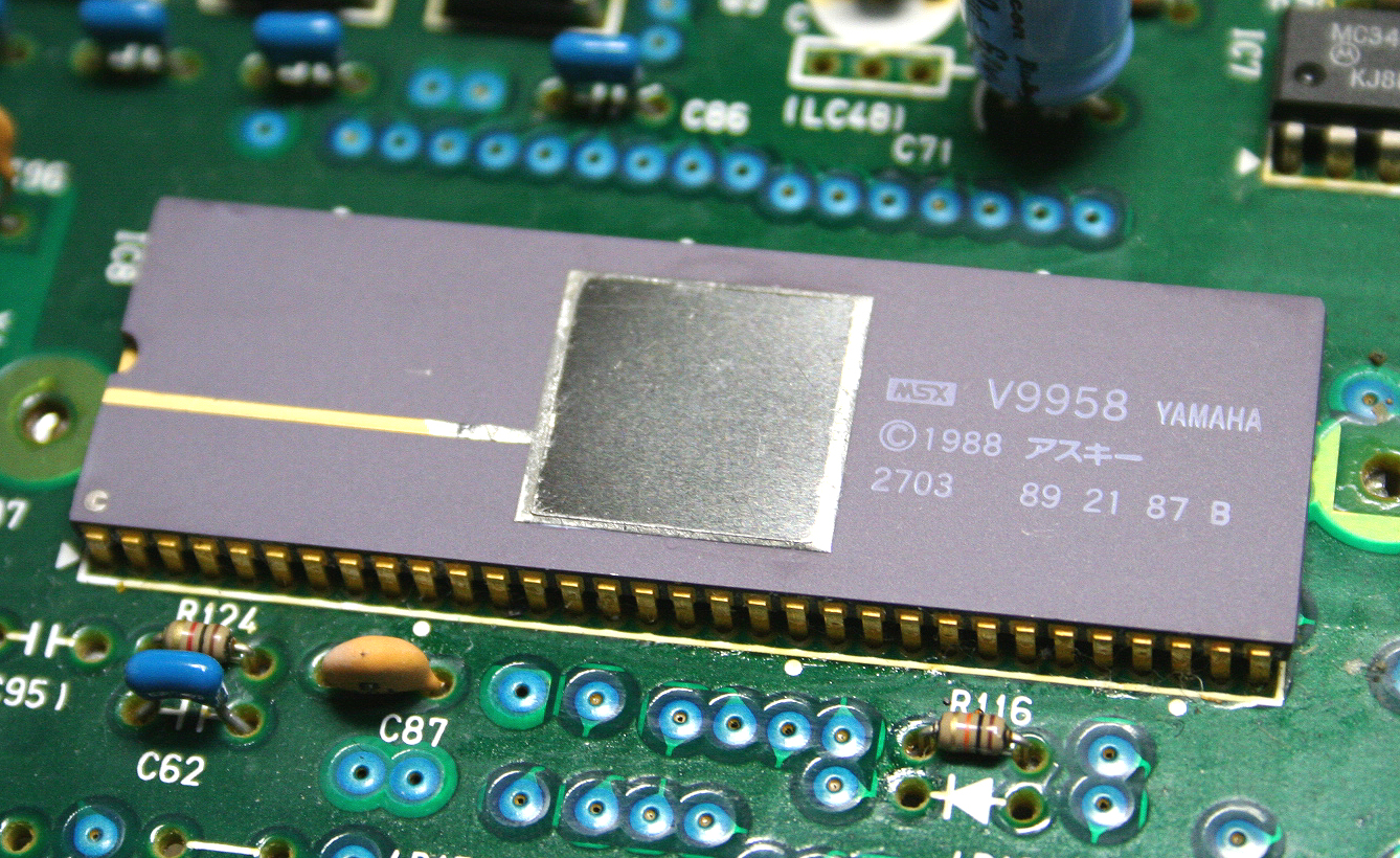
Browsing Wikipedia (as one does), I have stumbled upon this picture of a circuit board¹:
Now, when you look at it, there are several things that stand out as being interesting and different to today's commonly used PCB manufacturing techniques.
I don't have access to the board pictured, but here² are some more pictures of it. However I do recall seeing other circuit boards using these techniques; especially on lower-cost devices from the late 80s/early 90s and remote controls.
So, here is what I'd like to find more about:
Multiple soldermasks?
There seem to be at least two levels of soldermask. One of which is visible only around the vias, and the other opaque one covers and conceals stuff further.
What's the purpose of this second, very opaque layer?
-
To hinder reverse-engineering of the PCB layout. This however doesn't make that much sense to me, since the PCB pictured comes from an MSX computer, and AFAIK the MSX architecture was pretty much an open standard. Also, this additional opaque layer is absent on the bottom side.
-
Or is this not just an opaque soldermask, but that and another (rough) conductive layer over another (what you'd think of as traditional) soldermask; which would make some sense here too, perhaps for EMI shielding. Is this it? Another thing going for it is the large clearance around the vias.
-
Or is it something else entirely?
Blue vias
Don't the vias look interesting? How were those made? It seems that they did not use (now ubiquitous) plated through-holes manufacturing this board.
But what is this that they used instead and how were those made? Is this some sort of conductive epoxy?
The (relatively) large via size could be justified by it. It also seems like the material over the vias is rather concave with likely designed-in overlap over exposed copper around the hole. Were those filled-in one-by one?
Now, why did they use this method instead of the "modern" PTH? I suspect it must have been significantly cheaper for small enough number of holes. What would this method be called?
Searches for epoxy-filled vias do yield results, but of different-looking ones to this.
This is my first question here after all this time; I know however that having multiple sub-questions is sometimes frowned upon, but I hope this still counts as being reasonably related enough. Thank you for your answers.
I also hope some others find this as interesting, with the epoxy via technique perhaps finding another life in my homemade PCBs.
¹) Image taken from Wikipedia by Yaca2671. Wikimedia link
²) MSXinfo.net article on Panasonic FS-A1WX
 Clipping before soldering leaves a smaller solder blob than otherwise.
Best Answer
This appears to be a punched board (the outline and all the holes are punched in a single operation) with conductive liquid used to create vias. This is sometimes called STH (silver through hole) technology.
If you look at the holes where there is no via you can see that they are relatively rough and quite a bit larger than you might have for a drilled hole. This also helps speed assembly by minimizing accuracy requirements for machines or people.
Not sure about the solder mask appearance, maybe a second layer is applied (typically by screen printing) just to protect the vias.
My experience with this technology is that it's not all that reliable, especially in applications where a lot of vibration or shock is possible. It is very cheap per square meter because they can use low cost paper-based laminates and punch all the holes and outlines out of large panels in a single operation taking almost no time (on a cheap press too). Because the crappy cheap laminates are quite brittle (as anyone who has dealt with damaged cracked boards will attest to), they have to be heated in a batch before punching.
It was not all that uncommon in that era for factories to have quality problems with (what are now ubiquitous) plated through holes such as cracking around the holes, often caused by poor control of the various chemicals and processes involved, but those issues have mostly been vanquished.