I think you can't answer this with currents as above, instead you have to use charge flows, i.e. the drift of specific carrier populations.
Let's take an NPN transistor for example, with a supply connected between C and E to reverse-bias the CB junction.
At the micro level, what is ICBO composed of? Currents in reverse biased diodes are from random thermal creation of hole/electron pairs, so in this case we'd find new electrons being pulled out of the CB depletion zone and flowing to the collector, and new holes being pulled the other way and flowing into the base. Holes into the Base! There aren't electrons in that P-doped region to swallow the incoming holes, so they can diffuse through to the BE junction, meeting up with electrons, and reducing the BE depletion layer thickness, so forward-biasing that junction. (So, essentially the CB diode acts like a large resistor in series with the BE junction.)
But when the BE depletion zone narrows, the lowered barrier allows the vast population of mobile electrons in the Emitter to start crossing the junction into the Base region. So: small hole-flow from CB is turning on Vbe, causing large electron-flow coming from E. (This involves hfe, just as when Base is connected, where Ib produces a small hole-flow into BE junction, lowering Vbe and producing very large electron current Ie ~ hfe * Ib.)
Carriers flooding across BE junction. Electrons in the Base! Some will be swallowed by holes, but since the Base is thin and lighter-doped, most will diffuse across. When electrons arrive at the reverse-biased CB junction they're yanked across by the large e-field there.
Wouldn't this produce runaway, hfe*hfe*hfe...? Nope, and neither does runaway happen in diodes: forward biasing DOESN'T trigger even more forward biasing and so a runaway. It's because the BE junction is being forward biased by the holes (not electrons) coming from the Base region. The large amount of electrons pouring in from the Emitter region don't turn on the BE diode any more than it already is. Or in other words, Icbo is a hole-current just like Ib would be, and the large Ie doesn't reverse course while flipping its carrier polarity to make Icbo larger. Icbo and Ie are separate clouds of carriers flowing in the same piece of silicon. Icbo can "communicate with" the Ie via the BE junction-barrier and Vbe. But the two don't interact directly, in the simple case.
The thing you need to know is that the base is very thin/short.
So the electrons travel from emitter to base "thinking" it's a standard forward PN junction. However, like I said, the base is very small so many of the electrons end up at the collector side of the base and suddenly find themselves inside a big-#ss collector :-)
So there they all combine and form the collector current. Only few electrons make it out of the base without ending up in the collector, this explains the small base current.
So the base-collector junction itself isn't operating as if it is in reverse mode. It's not the junction causing the current, it is the base that is injecting carriers into the collector.

Best Answer
Removing R2 would increase the chances for thermal runaway, there are two "loads" on R1, one is R2 and the other is the transistor. If one "load" is removed than the voltage goes up. If R2 is removed then the voltage Vcb goes up and so does the current Ib. (you could also think of it from a current node perspective and the current through R1 must go through R2 and the transistor, if R2 is removed all the current goes through the transistor, which is a simple way to look at it but it sill works) This would increase current through the transistor because Ib would be higher and so would Ic.
But thermal runaway is independent of this. If you heat up a resistor, the resistance will change a bit (usually in ppm) but this normally doesn't produce a noticeable change in current.
The power dissipated in a transistor is based from Ic. So if you heat up a transistor, you get more current through the collector. This can be bad because this causes the part to heat up more, and more current to flow through, and more heat.
This is why it's important consider the thermal runaway effect and make sure you've considered the changes in beta over temperature. A good idea would to find the max temperature for the design in the datasheet and also consider what would happen if it increased Ic.
Here is an example of how current gain changes in a real transistor with temperature (the 2n3904). At certain currents (like 10mA) Ic would increase with the temperature increasing. The good thing is the designers accounted for the thermal runaway effects and at higher currents, beta/hFE goes down with temperature at higher currents which reduces the thermal runaway effect. In other BJT's, this may not happen. The most important thing is to avoid reaching the absolute maximum temperature of the part.
Edit:
I think the confusion is that for a PNP this would be true, since we have an NPN. If R2 is removed we have more Ib if R1 is the same in both circuits, more Ib means more Ic and more Ie. This would increase the temperature of the part and wouldn't necessarily cause thermal runaway but could cause thermal runaway by starting the cycle. It would depend on the parts in the circuit.
Now if we start from the circuit without R2 adding R2 would decrease the chances for thermal runaway.
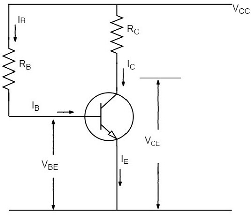
No portion of Ie (what you call Iceo) flows through R2 with an NPN. The directions of currents are indicated above.
No portion of Iceo flows through R2. All of Iceo flows through Re. All current in a transistor must exit through the emitter.