I was looking into various dc-dc converter designs, and I was interested in the split pi converter.
As a start, I just want to maximize the output voltage. I know in theory, the output voltage could be infinite, and in practice, it will be limited all the imperfections of the components I use. For now, I am just trying to better understand of how dc converters work. I have a basic understanding of how the buck and boost converters work, but I would really like to get a firm grasp on the split pi.
Also, would it be possible to get the same power transfer with BJTs as opposed to mosfets?
—100% speculation below this line—
I suspect there ought to be an optimum frequency that the transistors oscillate based on the capacitors and inductors used. I also suspect given an optimum transistor configuration, replacing some wires to the gates/bases of the transistors with resistors will yield an optimum configuration for for an arbitrary gain between input and output voltages. I also suspect that the ratio between certain pairs of these resistors will determine the gain of the system.
Best Answer
Summarised Solution:
Over 1 kV out from say 5 to 12V in if optimised for this purpose and your switches and output capacitor can handle it.
In real use, a few hundred volts would be doable but more than was sensible.
Long:
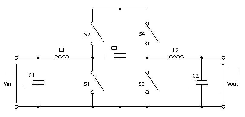
The split Pi is more complex than you need for what you say you want.
This is essentially a synchronous input, synchronous output full bridge boost buck converter used in many modern designs. It is fully bidirectional - ie it will convert any voltage at left to any sensible voltage at right OR can convert equally well in the reverse direction.
All you need to start is the parts up to C3. This is a standard boost converter. In non-synchronous versions S2 is replaced with an "upwards pointing" diode. (Parts to right of C3 will down convert the voltage on C3).
The available output voltage is "heaps" but in practice if maximum voltage was an aim you would place a second winding on L1 to provide a stepup ratio.
In real world use you could convert from say 12V to hundreds of volts as shown if necessary. The usual limits are the voltage ratings of L1, S1, S2, C3 (ignoring components beyond that).
In extreme cases the interwinding breakdown voltage if L1 becomes important (ask me how I know :-) ) with the voltage at the start of one winding and the end of the next being two layer voltages apart when windings are layed successively right to left then left to right. In some cases the voltage towards the winding ends can exceed the breakdown voltage of the wire insulation - making interwinding insulation important and how the wires are handled mechanically at the ends of each layer important. In most cases this is not an issue.
The absolute maximum output voltage occurs when the inductive energy in L1 is transferred into its stray capacitance. Consider:
Open all switches.
Close S1 until I in L1 is at a max.
Open S1 and DO NOT close any switch.
Voltage on L1 will now "ring" positively until the 0.5 x L1 x I^2 energy is stored in stray capacitance of L1 as 0.5 x Cstray x Vring^2.
So
With 12V in (or almost an Vin as Iin_max is what counts) this could be more than 1 kV in a carefully optimised case.
S1 and S2 are liable to object in most cases.