At some point in my life, I used to run the USB business for big semi company. The best result I remember was NEC SATA controller capable of pushing 320Mbps actual data throughput for mass storage, probably current sata drives are capable of this or slightly more. This was using BOT (some mass storage protocol runs on USB).
I can give a technical detailed answer but I guess you can deduce yourself. What you need to see is that, this is ecosystem play, any significant improvement would require somebody like Microsoft to change their stack, optimize etc, which is not going to happen. Interoperability is far more important than speed. Because existing stacks carefully cover the mistakes of slew of devices out there because when the USB2 spec come out probably the initial devices didn't really confirm to the spec that well since the spec was buggy, the certification system was buggy etc. etc.. If you build a home brew system using Linux or custom USB host drivers for MS and a fast device controller you can probably get close to the theoretical limits.
In terms of streaming, the ISO supposed to be very fast but controllers do not implement that very well, since 95% of the apps use Bulk transfer.
As a bonus insight, for example, if you go and build a hub IC today, if you follow the spec to the dot, you will practically sell zero chips. If you know all the bugs in the market and make sure your hub IC can tolerate to them, you can probably get in to the market. I am still amazed today, how well USB is working given number of bad software and chips out there.
does [ECC] mean you cannot use 10% of the available space on the card?
No. The ECC does not use any of the available user data space on the card.
Instead, the ECC is stored in separate "spare areas" next to the user data.
spare area
Many flash memory chips are designed such that, for each 512 byte sector intended for user data, there is an additional corresponding 16 byte "spare area". (Jim Cook. "Flash memory 101: An Introduction to NAND flash".)
Those spare areas, also called "out-of-band areas" (OOB areas), are designed to be used for ECC codes.
(Eureka Technology.
"NAND Flash FAQ".
"What is spare column in NAND flash?".
)
( Is flash chip capacity really limited to the powers of 2? )
In theory, a person could program the flash memory controller directly attached to these flash memory chips to use those "spare area" bits for whatever he wanted.
A few flash file systems directly connected to these flash memory chips use that "spare area" in sophisticated ways to store file system data and more complex error correction codes, instead of Hamming ECC data -- object IDs, wear-leveling data, etc. (Wikipedia: YAFFS).
(Compared to the simple "Hamming" system described below, such file systems have some other approach to detecting and dealing with bit errors -- Reed-Solomon codes, RAID-like multi-chip systems, or etc.).
SD/MMC cards have a tiny flash memory controller inside them, between the SD/MMC interface pins and the actual flash memory chips.
( see a b c for photos of SD card internals, showing the small controller chip and the much larger flash memory chip.).
ECC write
how come they can have such a high speed rating
When your computer or microcontroller sends the "write a 512 byte sector" command to the SD/MMC card, the sector is erased and then written.
There's not room here to discuss the things manufacturers do to make flash faster, so I'll stick to explaining why ECC cards are not noticeably slower than a (hypothetical) card without ECC.
My understanding is that all SD/MMC controllers should at least write Hamming ECC codes to the spare area for each block, unless they use use some more sophisticated error-correction system.
("ST AN1823: Error Correction Code in NAND Flash Memories")
(Is there some way to tell whether the card was really doing that or not?)
The flash memory chip is designed so the entire page (user data + spare area) is erased at once.
This erase would take the same amount of time on a flash chip without ECC, so the ECC doesn't slow erases down.
The controller calculates the ECC data, and blindly(*) writes the user data and the ECC data to the flash. Hamming codes can be calculated "at wire speed" while the user data is coming through the SD/MMC interface or while the user data is being sent to the flash card, so the ECC calculations don't slow the writes down.
The controller does have to write an "extra" 16 bytes of data for each 512 byte sector, but that is not noticeably slower than a hypothetical flash chip without ECC: 1/32 ~= 3% slower.
(*) SD card controllers don't bother reading back the data during a write to see if it worked.
They only detect problems much later, while handling a "read" command.
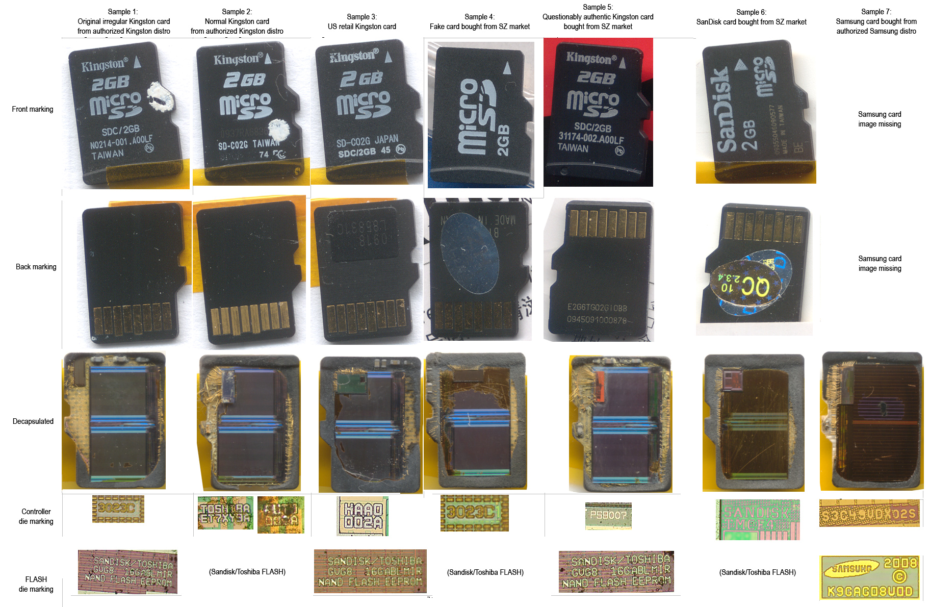
Alas, I hear rumors of unscrupulous people taking perfectly good 1 GB cards and reprogramming the controller into thinking there's actually 4 GB of flash connected to it.
The resulting fake/counterfeit/forged card seems to work fine for reads and writes until the first 1 GB is filled up; it even seems to work fine during (blind) writes to the rest of the "4 GB", but then things go horribly wrong trying to read data back from the card.
ECC read
a significant amount of time to recover errors ... because it needs to process the original data as a whole
Yes, Hamming codes needs to process the "whole block", but for SD cards the "whole block" is only 512 + 16 bytes.
When your computer or microcontroller sends the "read a 512 byte block" to the SD/MMC card,
the SD/MMC card controller reads the full 512 user bytes + 16 ECC bytes, corrects the errors (if there were any), and sends the corrected 512 bytes of user data to your computer or microcontroller
(or sends an error code if there were so many errors in the user data or in the ECC data or both that they were uncorrectable).
Because the on-card controller can read 512 + 16 bytes from the flash and do Hamming correction much faster than it trickles response codes and data through the card interface, this is not noticeably slower than a (hypothetical) card without ECC.
As far as I know, SD/MMC cards don't use Reed-Solomon error correction -- but I suppose they could do that internally, and there's no way to tell from the outside.

Best Answer
What is the physical representation of bits being sent? In many cases, intra-packet error-correcting codes will be useless because even a transient glitch will cause many bits to be misinterpreted--quite possibly all bits until the next synchronization mark.
If forward error correction is needed, and packets are of uniform size, the simplest approach may be to send n packets worth of data using n+1 packets--each labeled with a packet number--where the (n+1)th packet contains the xor of the other ones. If the first n packets are read successfully, ignore the extra one. Otherwise, if one packet is missing or corrupted, infer its value by xor'ing the remaining n packets together.
A slight improvement of this approach would be to send 2n packets worth of data using 2n+2 packets, interleaving two sets of n+1 packets, each set being formulated as above. That would guarantee recovery from any single communications glitch which was no longer than the time required to send a single packet (a short glitch might hit the end of one packet and the start of the next, but the two packets would be in different xor-groups).
The biggest limitation with this approach is that packets must be assembled into groups (or, putting it another way, what could otherwise be larger packets must be subdivided into smaller ones). On the other hand, it is robust against glitches that would cause synchronization loss render large amounts of data unreadable.