I am designing a electrical device for a research project (I'm a PhD student, but unfortunately not EE!). More info on the device can be found at http://iridia.ulb.ac.be/supp/IridiaSupp2012-002/
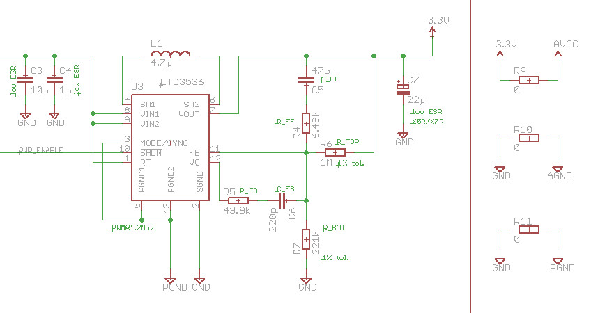
The last prototype had a problem with the power supply, and thus I tried to overcome the problems by designing a new and better one. As the device is powered by a Lithium-Ion battery, I decided to use a LTC3536 buck/boost switching regulator: http://cds.linear.com/docs/en/datasheet/3536fa.pdf
I basically used the reference implementation (page 1 of the datasheet) for a 1A/3.3V power supply as seen here:

(source: ulb.ac.be)
There are three separate ground planes: PGND, coming from the battery, GND, the normal ground, and AGND for analog sensors etc.
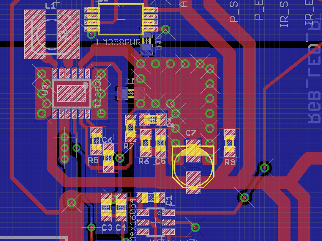
This is the board as I designed it in Eagle. I already noticed some deviations from the reference design, for example, C3 and C4 should be places a lot closer to the LTC (U3):

(source: ulb.ac.be)
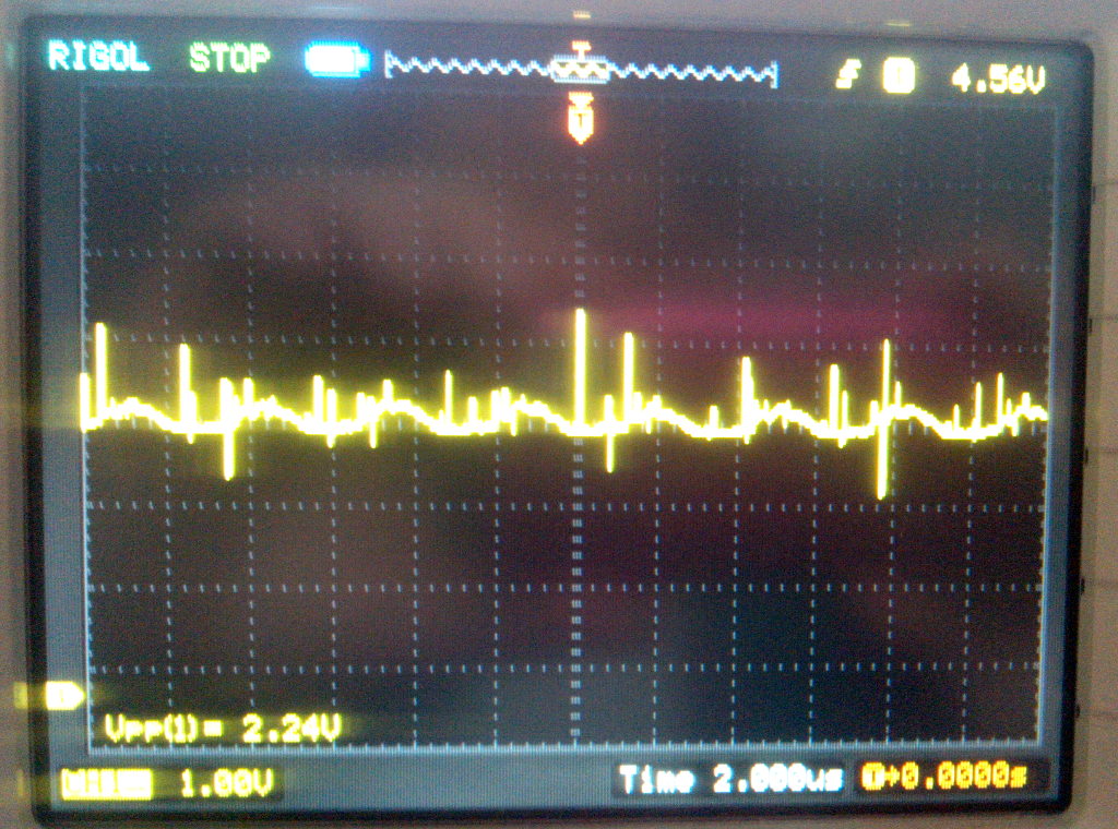
This is the output that I see on VCC (with or without load, Vin=4.7V)
As you can see, Vpp is huge! It's smaller for Vin<4.3V, but still quite substantial.

(source: ulb.ac.be)
I did a bit of trial-and-error by moving C3 and C2 closer to the LTC, and adding in another 1µF cap to C7. This didn't help much. I then replaced C7 with a 220µF cap instead of the 22µF mentioned in the datasheet. With this, Vpp is ~200mV. This is a lot better but still a long way from what is specified in the datasheet. Additionally, this is only the case for Vin>4.3V; below this threshold Vpp is still over 2V. I guess it's the boost vs. the buck regulation that makes the change, but I don't really see how I can correct it.
Now the questions:
- I was wondering if I made a mistake that is obvious to the trained eye?
- Why is Vpp so huge, when the noise given in the datasheet is only 40mV?
- Is there another way to fix this other than randomly dropping in different output capacitors?
Best Answer
I think you'll have problems with your layout. C3/C4 MUST be closer to pin 1 (EDIT this should read pins8/9 not pin1). When I say closer I mean living on it! Ditto C7 - it needs to be camped right on pin 7. Now I've never used this part but this is standard procedure for this type of device.
Think about the current pulses flowing from pin 7 to C7 and the length of track between it and the IC - probably 20nH of track.
The ground return of C7 - where is it going? It's going right back to the wrong ground pin (signal ground). C7's ground should be as short as possible to pins 5 and 13 as possible without breaking trespass laws. And this should be your star-point for keying off signal ground. Signal ground should then go to your feedback components and not pass any load or C7 current at all.
I would decline testing this PCB if it was handed to me. Sorry for being abrupt but these are golden rules on switching circuits: -