All digital ICs should have decoupling caps between their power and ground pins. These should be ceramic and physically as close as possible to the IC. You want to minimize the loop length from power pin to cap to ground pin thru the IC and back to the power pin.
Decoupling caps deal with short term current spikes the IC draws. They must therefore be high frequency. Large capacitance is not necessary, and since large capacitors usually have poor high frequency response, they are worse. A 100µF electrolytic cap is pretty useless for decoupling. 1µF to 100nF ceramic is good.
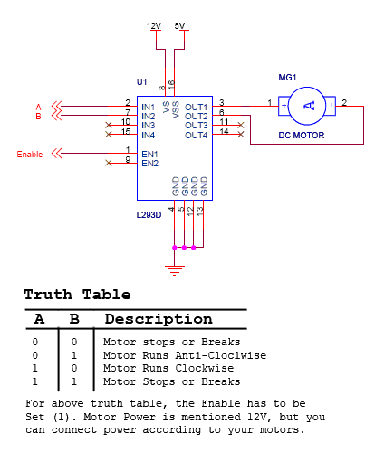
As for the cap on the motor, the idea is good but I think 100nF is too large. That could cause excessive or unnecessary current to flow in the H bridge every time it switches. If you're only reversing motor direction occasionally, then this isn't a big deal. If you're using the H bridge to modulate the apparent motor drive with PWM, then you should lower the cap. Something like 1nF should still cut down the noise the motor is making while not getting in the way of switching.
What's the problem?
It isn't clear why you can't use your existing layout and just translate for the bigger package?
Guard rings are about DC...
The guard ring is designed to deal with leakage currents by placing a nearby intermediate voltage between sensitive sources.
The ground plane is for providing the low-inductance return path. If you are moving (returning) a substantial percentage of your signal on the guard ring, something is wrong.
Terminating your guard ring is not a hugely complicated concern, so don't over-think it.
Bypass what exactly?
The load capacitors/oscillator do not need an additional bypass. It doesn't do anything because there is nothing to bypass here.
The power loop for the oscillator includes the power entry pin to the PIC (bypass there), it's internal power distribution grid, the oscillator driver circuits, the oscillator tracks, and the crystal/osc itself.
Your bypass cap at the bottom of the second figure doesn't influence anything in that pathway. The answer you cite deals with a completely different scenario (the power pins of the IC itself, not I/O pins as in your scenario).
What to do:
- Single via at the extremity of the guard ring to ground plane
- Keep the crystal/osc lines as short as possible
- Place the load caps next to the crystal/osc -- turning them so that they are parallel to the long side of the crystal/osc with their ground pins facing each other is a good way to lower inductance, but it isn't critical to do so.
- Pour a small surface ground plane over the ground pads (don't forget thermal relief) and stich to the ground plane underneath with a few vias.
- Escape the nearby PIC pins via fanout and via to the lower surface for further travel (allows the lines to take up less y-space so that the crystal can be placed closer to the chip)
- Regarding C10 in the original figure. Just place it as close to (what looks like to me) pin #38 as possible. Don't worry about a cap near pin #41. It's covered by C10 even if C10 is a little further away.
Good luck! I'll follow-up if you have any further questions. Cheers.


Best Answer
You probably want the cap on (or near) the motor. The main purpose of the cap, there, is not to protect anything from ripple current, since neither the motor nor (probably) the output side of the IC, is particularly sensitive to it, but rather to reduce the stray rf caused by the commutation of the motor. Placing the capacitor near the motor means only a short region of the leads between the driver source and the motor is experiencing much ripple, and so there's less rf interference.
As for other places to use smoothing capacitors, the best option is to just hook everything up, turn it all on, and probe around sensitive areas (IC signal and power inputs, mainly) with an Oscilliscope and add enough capacitance to drop undesirable ripple to a few millivolts (or whatever the circuit requires).